


Other Technologies
The Office of Technology Transfer facilitates the licensing and distribution of diverse technologies that support various technological needs.
OTT case 22-002 | Patent pending
The market for electric powered bicycles (a.k.a. ebikes) is currently exploding. Ebikes enable riders to start up the hobby of biking or commute to work without risk of being too strenuous and allows older people to take longer excursions due to the electrical assistance with climbing hills. Dozens of manufacturers have introduced products to the market to address these needs, with prices ranging from ~$600 (e.g. Walmart models) up to ~$5-6k for high-end models designed for aggressive off-road applications.
This patent pending invention is a bicycle trailer designed for comfortable passenger riding while reducing the workload for the bicycle rider, enabling tandem adventures when one rider is disabled or otherwise unable to ride a bike. The design utilizes an “off-the-shelf” ebike conversion kit that is reconfigured onto a trailer frame. The trailer includes an onboard battery, control system, motorized wheel, and headlight. Meanwhile, the controls for the electric system are mounted onto the pilot bicycle including a pedal-assist sensor, throttle, and display. In this manner, the pilot rider has control over the power delivered by the trailer to assist with propulsion. Since typical bicycle trailers do not include a suspension system, the ride would typically be very rough for a passenger. This ebike trailer is based on a patent-pending first-class lever suspension system (see OTT case 21-022), ensuring a smooth, shock-free ride while minimizing any leaning of the trailer during cornering.
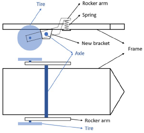
OTT case 21-022 | Patent pending
When an uneven load is biased toward one side of a trailer, the reaction spring on the overweighted side will proportionally depress, causing the overweight side to sag. This effect can result in trailers that lean to one side when either loaded unevenly, or when the trailer is pulled around a sharp corner at highway speeds. This leaning affect introduces potential turnover risk to the load or reduces the loading capacity of the trailer, particularly with taller loads or those with uneven weight distributions. Researchers at U of I have invented an integrated trailer suspension design that provides an optimum combination of load balancing stability while maintaining the smooth-riding benefit of traditional trailer systems. The design utilizes a first-class lever to engage each suspension spring, and ties both sides of the trailer together for load balancing.
The figure depicts a simplified illustration of this hybrid suspension system. Each side of the trailer includes a first-class lever (Rocker arm) that reacts the tire load from the ground to a compression spring mounted on the outside of the frame. Both rocker arms are solidly linked together via the axle. As a result, when an uneven load is applied, both rocker arms act in unison to distribute the load evenly across both springs, resulting in increased stability. The trailer axle also functions as a torsional spring between each side of the system to enable each side to react independently to obstacles, thus keeping the smoother ride.
OTT Case 20-021 | patent pending
The invention relates to the development of a unique, fully controllable, high speed, high-pressure, variable volume, reactor known as a Rapid Compression Expansion Machine (RCEM). The RCEM is used for studying chemical kinetics and is capable of an infinitely variable compression ratio up to 20, high positioning accuracy, and fully programmable piston speeds over 5 meters per second. The utility of this device has been demonstrated in a study involving reactivity build up during the ignition chain reaction sequence for transportation fuels and aid in the development of advanced engine concepts such as the homogeneous charge compression ignition engine (HCCI). The tracking of the intermediates during the pre-ignition phase as a function of time is a very challenging task due to the rapidity and explosive nature of combustion reactions. The developed RCEM can easily accomplish this in a very repeatable and programmable fashion. The device well suited for studying general reaction kinetics in the premixed gases, aerosols/dusty mixtures, and sprays environments.
OTT case 16-015 | U.S. utility patent 10,347,976
Unmet Need
Antennas have found numerous applications, especially in wireless network, near field communication, 3D integration, next generation data storage, etc. While the recent developments in antennas is attributed by low power, smaller size, and interface facility, the realization of complex antenna design and fabrication using cost efficient printed circuit board (PCB) technology is less explored. The current state of art utilizes techniques like Low Temperature Cofired Ceramic (LTCC) that is costly. PCB stacking techniques used with success for design of small wireless sensor nodes has opened a new avenue in designing cost efficient 3D antennas.
Invention Description
Researchers at the University of Idaho have developed a novel hemispherical antenna design that utilizes stacks of two-layer printed circuit boards to create the 3D hemispherical structure. The novel approach overcomes the implementation and fabrication challenges faced by the current state of art by leveraging PCB technology. This method provides simplified alternatives to wire based fabrication methods to realize complex antenna geometries. The novel approach offers considerable cost savings over the Low Temperature Cofired Ceramic (LTCC) technology, which is 20 times the costs of PCB based designs.
Market Potentials/Applications
- Smart Antenna for mobile devices
- Consumer electronics
- Smart Grids
- 3D Integrated circuits
- Wearable electronics
- Wireless networks
Key Benefits/Advantages
- Cost efficient approach to create 3D hemispherical structure.
- Smaller form factor
- Reduced size compared to wire base antenna
- Reduces overall cost
- Need not remove copper layers below the antenna as compared to ceramic chip antenna
Development Stage
Tested
IP Status
Provisional
OTT case 13-001 | U.S. utility patent 10,351,455
Called N-E-W™ (Nutrient, Energy, Water), this technology uses metal functionalized biochar as a sacrificial catalyst with ozone for catalytic oxidation. N-E-W Tech™ can take many dirty waters to a level of treatment required for unrestricted reuse and recycling. Catalytic oxidation allows for destructive removal of most organic contaminants (it can mineralize them to carbonates) and sterilizes water (kills all microbial life including prions, viruses and bacterial spores). Mineralized nutrient phosphorus and nitrogen are bound to the biochar and recovered from the water. The nutrient-laden biochar can be recovered and pelletized for fertilizer use and as a soil amendment in agriculture.
OTT Case 12-028 | U.S. utility patent 9,691,556
Researchers in the University of Idaho developed an electrochemical device, comprising a positively charged electrode; a negatively charged electrode; a graphene layer comprising graphene having a substantially micro-crystalline grain size ranging from about 2 nm to about 15 nm, basal planes that are substantially planar, and a total electrochemical window of from at least about 3 V to about 5 V; and an electrolyte. In particular embodiments, the graphene layer covers at least a portion of the positive electrode, the negative electrode, or both. The electrochemical device can be connected to a power source. In some embodiments, the electrochemical device can be used to store energy or to provide energy. The graphene layer is capable of providing a capacitance ranging from at least 200 μF/cm2 to about 700 μF/cm2.
OTT Case 12-009 | U.S. utility patent 9,360,380
Streambed morphology is in constant evolution, causing scour and deposition processes. These processes affect engineering structures such as bridge piers, levee foundations, apron footings and ecological processes in addition to restoration, enhancement and improvement projects for streams and rivers. Monitoring streambed evolution over time is an essential component of river and watershed management. Limitations of current technology are the cost and difficulty of deploying a large array of sensors so that the distributed erosion-deposition pattern can be obtained. Researchers at the University of Idaho have developed a new scour-deposition instrument that is both a low-cost and real-time sensor. In addition to monitoring scour-deposition in real time, this sensor would have applications for quantifying streambed sediment thermal properties, benthic thermal regime and for monitoring connectively between stream and aquifer.
Figure depicts a prototype senor fitted with four temperatures probes (silver bands).