


FIB/SEM Laboratory Services and Rates
DB-FIB/SEM Lab operates under following hourly rates that were approved by the Service Center Rate Commission of the University of Idaho.
| Services | Academic (U of I) | Academic (non-U of I) | Corporate |
|---|---|---|---|
| SEM | $75 | $95 | $175 |
| FIB+SEM | $175 | $275 | $375 |
| EBSD/EDS Detector* | $35 | $55 | $100 |
| Technician Assistance | $25 | $25 | $50 |
| TEM Sample Preparation | Call | Call | Call |
* EDS or EBSD rate is an addition to the listed SEM or FIB+SEM hourly user rates.
Please review the instrument request form (PDF) before contacting us at 208-885-1063 or fibsem@uidaho.edu for available dates and time of operations.


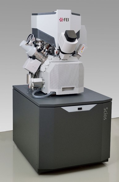
FEI SCIOSTM
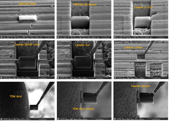
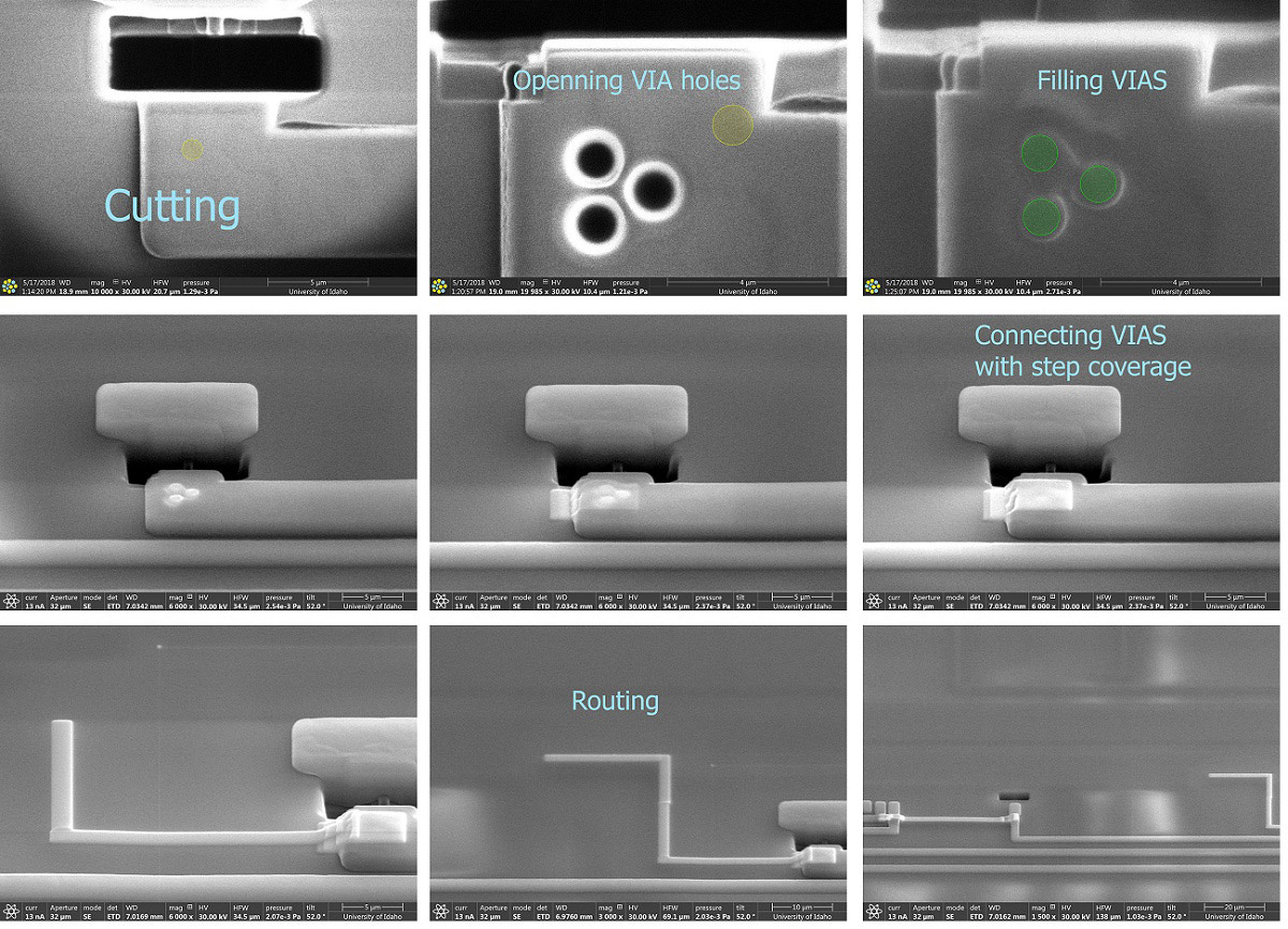
FEI/Thermo Scientific SciosTM is the most versatile high-resolution SEM/FIB for 2D and 3D material characterization and analysis with EasyLift EX NanoManipulator for in-situ sample manipulation and TEM lamella transfer. The instrument combines innovative electron and ion optics with state of the art patterning control. This combination expands the characterization and analytical capabilities by providing better and faster ways for material characterization, analysis and sample preparation.
Our Scios is equipped with Gold (Au) and Platinum (Pt) sources for deposition.
Watch 15 minutes introductory FEI Scios Discovery video
Electron Optics (SEM)
The main elements of the electron optical system are:
Source
- Field emission gun assembly with Schottky emitter source.
- The assembly is optimized for high brightness/high current, providing low-noise imaging.
- The pre-alignment of the FEG ensures no mechanical alignment is required.
- Easy gun installation and maintenance is provided with Auto bake-out and Auto Start capabilities.
Objective Lens
- Dual Objective combining field-free magnetic and electrostatic lenses, with a 60 degree geometry
Voltage:
- 200 eV to 30 keV
- 20 eV landing energy possible with optional Beam Deceleration
Beam Current:
- 1 pA to ≥200 nA
Resolution: (at Optimum working distance)
- 0.8 nm at 30 kV (STEM)
- 1.0 nm at 15 kV (Trinity)
- 1.6 nm at 1 kV (Trinity) at eucentric working distance
- 2.5 nm at 1 kV (Trinity)
Ion Optics (FIB)
The main elements of the ion optical system are:- Field emission focused ion beam optics with liquid Gallium ion emitter.
- Source lifetime: >1000 hours
- Voltage: 500 V to 30 kV
- Beam current: 1.5 pA - 65 nA in 15 steps
- Resolution: 5.0 nm @ optimum working distance
Scanning system
- High-resolution digital scanning engine controlled from the User Interface.
- Pixel density 768 x 512, 1536 x 1024, 3072 x 2048, 6144 x 4096, selectable
- Minimum dwell time 25 ns/pixel; maximum 25 ms/pixel
- Electronic scan rotation by n x 360 degrees
Patterning (Milling) system
- High-resolution digital patterning engine controlled from the User Interface
- Maximum resolution: 64k x 64k
- Minimum Dwell Time: 25 ns/pixel
- Maximum Dwell Time: 25 ms/pixel
- Multiple standard pattern shapes and recipes, including annular milling
- Variable dwell time pattern to give 3D milling
- Complex milling patterns through Bitmap import, dynamic threshold milling, array generation, exclusion zones and polygon building
Detection
- A secondary electron detector (Everhardt-Thornley SED)
- The Trinity detection system is comprised of:
- A segmented, lower in-lens detector (T1),
- An upper in-lens detector (T2)
- An optional in-column detector (T3)
- An integrated IR-CCD camera is standard for in-chamber viewing

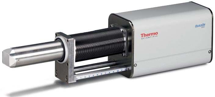
Thermo QuasOrTM EBSD Detector
Our Electron Backscattered Detection (EBSD) system composes of a 600fps Thermo QuasOr EBSD detector with integrated motorized slide. System includes Basic and Advanced level EBSD software for Acquisition, Euler, Phase Mapping, Concurrent Spectral Imaging, Grain Size Analysis, CSL and special boundary mapping.
The detector is connected to Noran System 7 Spectral Acquisition and Imaging System.

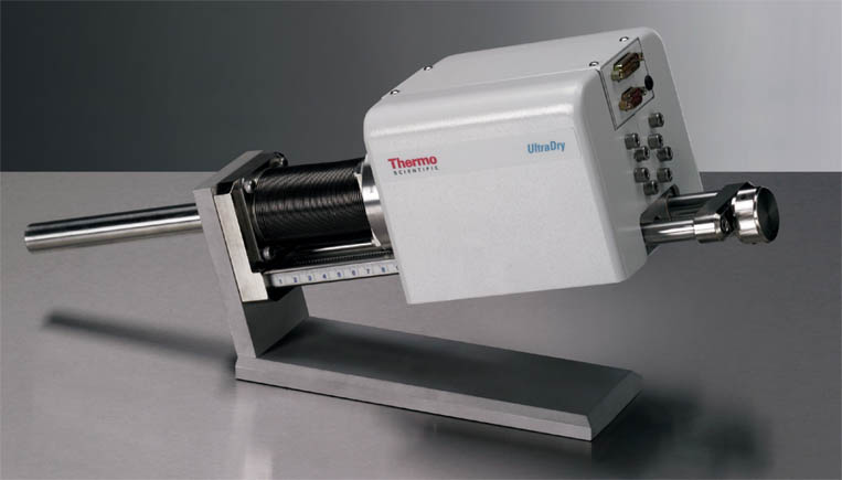
Thermo UltraDryTM EDS Detector
UltraDry Premium EDS Detector is with NORVAR® light element window, 30mm2 sensor, 129eV resolution (Mn) and guaranteed sensitivity down to beryllium.
Our EDS detector is connected to Noran System 7 Spectral Acquisition and Imaging System.

Noran System 7 Spectral Acquisition and Imaging System
Noran 7 includes digital acquisition electronics, spectral imaging software, standardless or full standards quantitative analysis, ZAF, Proza, and Cliff Lorimer matrix corrections, digital electron image and X-ray map acquisition, quantitative mapping and dynamic smart display, Point and Shoot image interrogation, over 16 automatic processing functions (with manual override preference), and Microsoft Word® for report generation.
Noran 7 also have Direct to Phase Software for extraction, display, and Principle Component Analysis (PCA) of Spectral Images and X-ray maps to determine and identify major phases and compounds. It also includes Compass (PDF), XPhase (PDF), and Match (PDF) options.